
NOTE: For detailed information on purchasing options, contact your
local Allegro field applications engineer or sales representative.
Allegro MicroSystems, Inc. reserves the right to make, from time to time, revisions to the anticipated product life cycle plan for a
product to accommodate changes in production capabilities, alternative product availabilities, or market demand. The information
included herein is believed to be accurate and reliable. However, Allegro MicroSystems, Inc. assumes no responsibility for its use; nor
for any infringements of patents or other rights of third parties which may result from its use.
Recommended Substitutions:
BiMOS II Latched Drivers
A5800 and A5801
For new customers or new applications, refer to the
6800
and
6801
.
Date of status change: May 2, 2005
Deadline for receipt of LAST TIME BUY orders: October 28, 2005
These parts are in production but have been determined to be
LAST TIME BUY. This classification indicates that the product is
obsolete and notice has been given. Sale of this device is currently
restricted to existing customer applications. The device should not be
purchased for new design applications because of obsolescence in the
near future. Samples are no longer available.
Last Time Buy

UCN5800A
BiMOS II LATCHED DRIVERS
UCN5800L
Always order by complete part number, e.g.,
UCN5801EP .
The UCN5800A/L and UCN5801A/EP/LW latched-input BiMOS ICs
merge high-current, high-voltage outputs with CMOS logic. The CMOS
input section consists of 4 or 8 data (`D' type) latches with associated com-
mon CLEAR, STROBE, and OUTPUT ENABLE circuitry. The power
outputs are bipolar npn Darlingtons. This merged technology provides
versatile, flexible interface. These BiMOS power interface ICs greatly benefit
the simplification of computer or microprocessor I/O. The UCN5800A and
UCN5800L each contain four latched drivers; the UCN5801A, UCN5801EP,
and UCN5801LW contain eight latched drivers.
The UCN5800A/L and UCN5801A/EP/LW supersede the original
BiMOS latched-input driver ICs (UCN4400A and UCN4801A). These
second-generation devices are capable of much higher data input rates and
will typically operate at better than 5 MHz with a 5 V logic supply. Circuit
operation at 12 V affords substantial improvement over the 5 MHz figure.
The CMOS inputs are compatible with standard CMOS and NMOS
circuits. TTL circuits may mandate the addition of input pull-up resistors.
The bipolar Darlington outputs are suitable for directly driving many periph-
eral/power loads: relays, lamps, solenoids, small dc motors, etc.
All devices have open-collector outputs and integral diodes for
inductive load transient suppression. The output transistors are
capable of sinking 500 mA and will withstand at least 50 V in the OFF state.
Because of limitations on package power dissipation, the simultaneous
operation of all drivers at maximum rated current can only be accomplished
by a reduction in duty cycle. Outputs may be paralleled for higher load
current capability.
The UCN5800A is furnished in a standard 14-pin DIP; the UCN5800L
and UCN5801LW in surface-mountable SOICs; the UCN5801A in a 22-pin
DIP with 0.400" (10.16 mm) row centers; the UCN5801EP in a 28-lead
PLCC.
FEATURES
s
To 4.4 MHz Data Input Rate
s
High-Voltage,
High-Current Outputs
s
CMOS, NMOS,
TTL Compatible Inputs
s
Output Transient Protection
s
Internal Pull-Down Resistors
s
Low-Power CMOS Latches
s
Automotive Capable
2
3
4
5
6
7
8
9
10
11
12
13
14
SUPPLY
GROUND
CLEAR
OUT
1
OUT
2
OUT
3
Dwg. PP-014A
OUT
4
1
14
1
COMMON
OUTPUT
ENABLE
IN
1
STROBE
IN
2
IN
3
IN
4
V
DD
LATCHES
Data Sheet
26180.10B*
ABSOLUTE MAXIMUM RATINGS
at +25
�
C Free-Air Temperature
Output Voltage, V
CE
. . . . . . . . . . . . . . 50 V
Supply Voltage, V
DD
. . . . . . . . . . . . . . 15 V
Input Voltage Range,
V
IN
. . . . . . . . . . . -0.3 V to V
DD
+ 0.3 V
Continuous Collector Current,
l
C
. . . . . . . . . . . . . . . . . . . . . . 500 mA
Package Power Dissipation,
P
D
. . . . . . . . . . . . . . . . . . . . See Graph
Operating Temperature Range,
T
A
. . . . . . . . . . . . . . . . -20
�
C to +85
�
C
Storage Temperature Range,
T
S
. . . . . . . . . . . . . . . -55
�
C to +150
�
C
Caution: CMOS devices have input static
protection but are susceptible to damage when
exposed to extremely high static electrical
charges.
Note the UCN5800A (DIP) and the UCN5800L
(SOIC) are electrically identical and share a
common terminal number assignment.
5800
AND
5801
5800
AND
5801
BiMOS II
LATCHED DRIVERS
115 Northeast Cutoff, Box 15036
Worcester, Massachusetts 01615-0036 (508) 853-5000
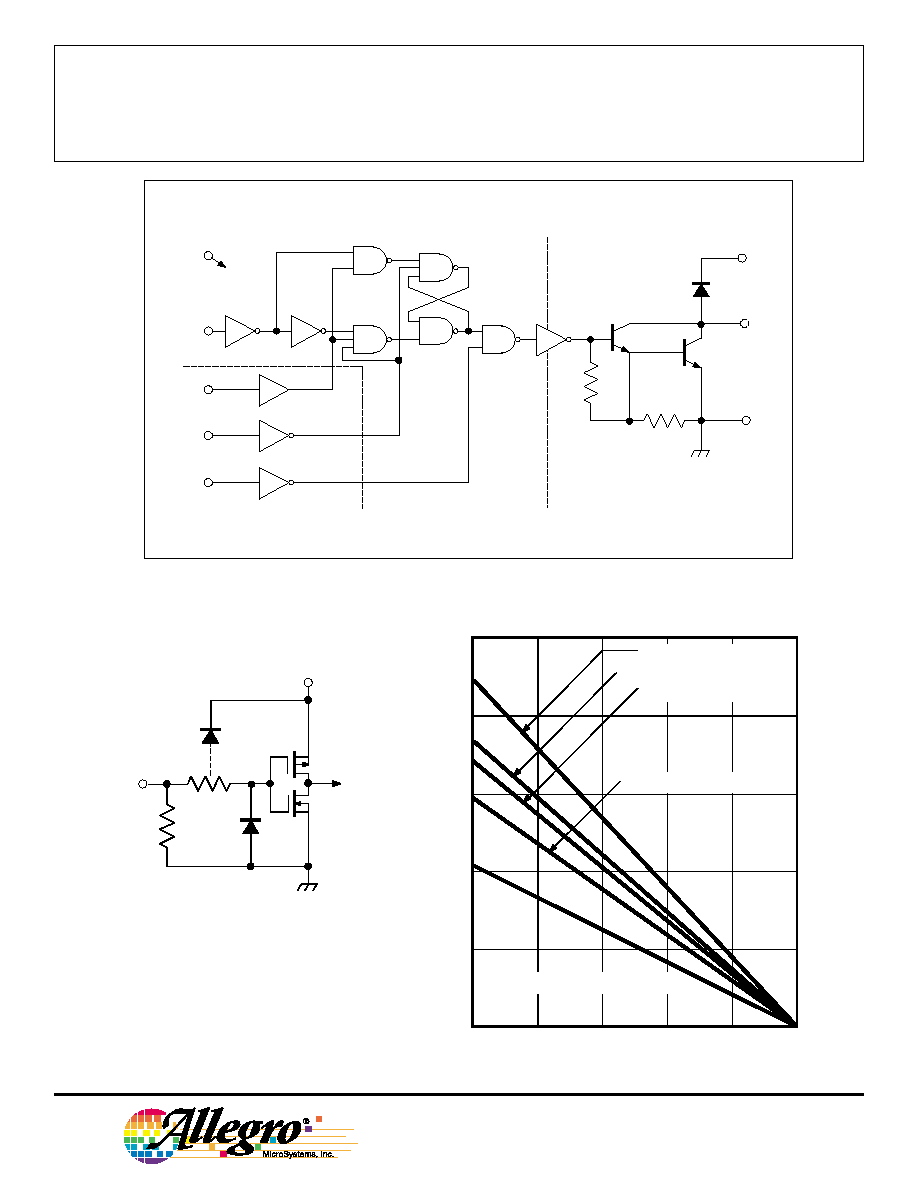
FUNCTIONAL BLOCK DIAGRAM
Copyright � 1985, 2002 Allegro MicroSystems, Inc.
50
75
100
125
150
2.5
0.5
0
ALLOWABLE PACKAGE POWER DISSIPATION IN WATTS
AMBIENT TEMPERATURE IN
�
�
�
�
C
2.0
1.5
1.0
25
Dwg. GP-023-1A
22-PIN DIP, R
JA
= 56
�
C/W
28-LEAD PLCC, R
JA
= 68
�
C/W
14-PIN DIP, R
JA
= 73
�
C/W
14-LEAD SOIC, R
JA
= 120
�
C/W
24-LEAD SOIC, R
JA
= 85
�
C/W
COMMON
GROUND
STROBE
OUTPUT ENABLE
IN
N
COMMON MOS CONTROL
TYPICAL MOS LATCH
TYPICAL BIPOLAR DRIVE
OUT
N
Dwg. FP-016-1
CLEAR
SUPPLY
V
DD
TYPICAL INPUT CIRCUIT
Dwg. EP-010-4A
IN
V
DD

5800
AND
5801
BiMOS II
LATCHED DRIVERS
ELECTRICAL CHARACTERISTICS at T
A
= +25
�
C, V
DD
= 5 V (unless otherwise noted).
Limits
Characteristic
Symbol
Test Conditions
Min.
Typ.
Max.
Units
Output Leakage Current
I
CEX
V
CE
= 50 V, T
A
= +25
�
C
--
--
50
�
A
V
CE
= 50 V, T
A
= +70
�
C
--
--
100
�
A
Collector-Emitter
V
CE(SAT)
I
C
= 100 mA
--
0.9
1.1
V
I
C
= 200 mA
--
1.1
1.3
V
I
C
= 350 mA, V
DD
= 7.0 V
--
1.3
1.6
V
Input Voltage
V
IN(0)
--
--
1.0
V
V
IN(1)
V
DD
= 12 V
10.5
--
--
V
V
DD
= 10 V
8.5
--
--
V
V
DD
= 5.0 V (See Note)
3.5
--
--
V
Input Resistance
r
IN
V
DD
= 12 V
50
200
--
k
V
DD
= 10 V
50
300
--
k
V
DD
= 5.0 V
50
600
--
k
Supply Current
I
DD(ON)
V
DD
= 12 V, Outputs Open
--
1.0
2.0
mA
V
DD
= 10 V, Outputs Open
--
0.9
1.7
mA
V
DD
= 5.0 V, Outputs Open
--
0.7
1.0
mA
I
DD(OFF)
V
DD
= 12 V, Outputs Open, Inputs = 0 V
--
--
200
�
A
V
DD
= 5.0 V, Outputs Open, Inputs = 0 V
--
50
100
�
A
Clamp Diode
I
R
V
R
= 50 V, T
A
= +25
�
C
--
--
50
�
A
V
R
= 50 V, T
A
= +70
�
C
--
--
100
�
A
Clamp Diode Forward Voltage
V
F
I
F
= 350 mA
--
1.7
2.0
V
NOTE: Operation of these devices with standard TTL or DTL may require the use of appropriate pull-up resistors to ensure a minimum logic "1".
Saturation Voltage
Leakage Current
(Each
Stage)
(Total)
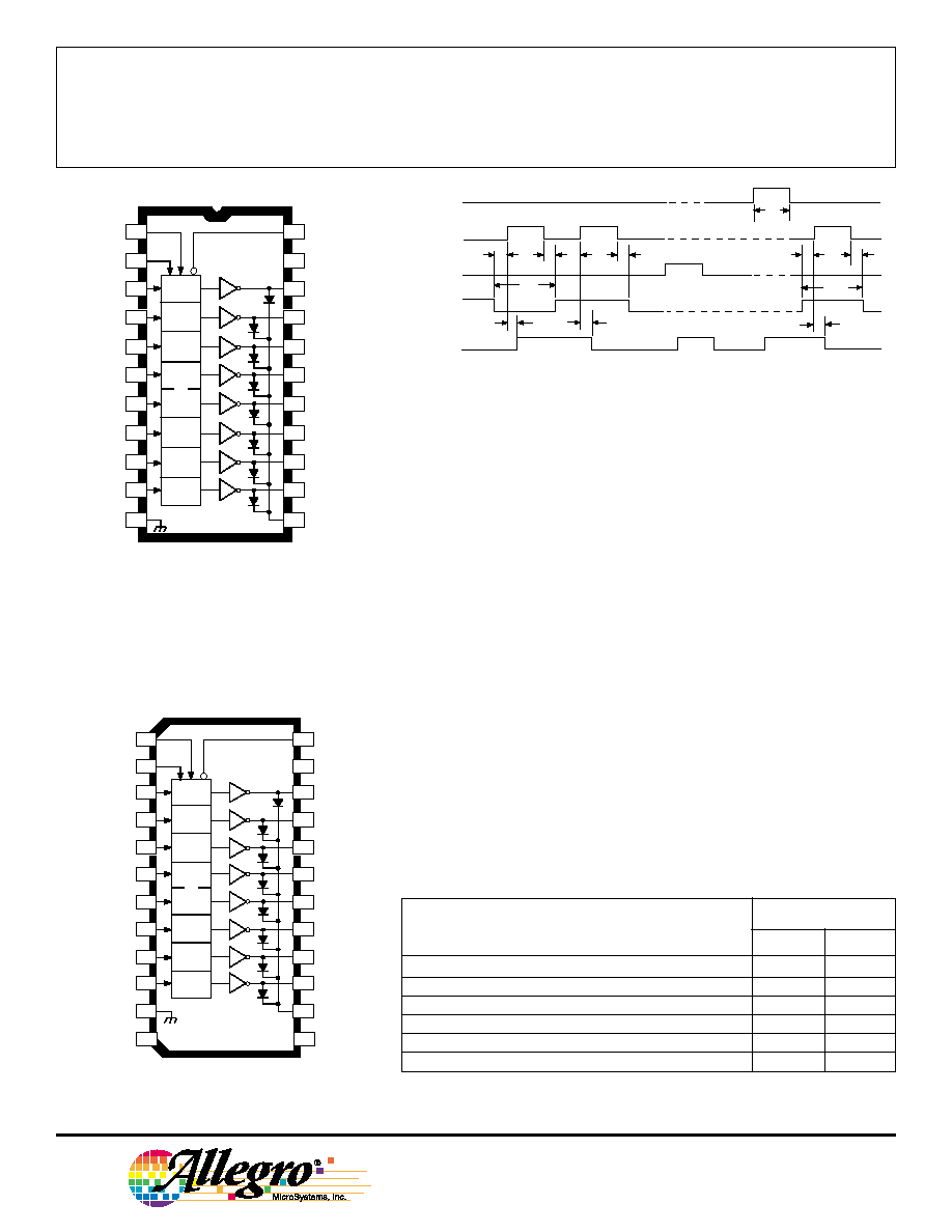
1
2
3
4
5
6
7
8
9
10
11
12
13
14
15
16
17
18
19
20
21
22
23
24
25
26
27
28
GROUND
OUTPUT
ENABLE
STROBE
K
ST
V
DD
OE
Dwg. PP-037
LATCHES
NC
NC
NC
NC
NC
NC
SUPPLY
LAMP DIODE
COMMON
C
CLEAR
OUT
1
IN
8
OUT
8
OUT
2
OUT
3
OUT
4
OUT
5
OUT
6
OUT
7
IN
1
IN
2
IN
3
IN
4
IN
5
IN
6
IN
7
UCN5801EP
(additional pinout diagrams
are on next page)
5800
AND
5801
BiMOS II
LATCHED DRIVERS
115 Northeast Cutoff, Box 15036
Worcester, Massachusetts 01615-0036 (508) 853-5000
TRUTH TABLE
OUT
N
IN
N
STROBE
CLEAR
ENABLE
t-1
t
0
1
0
0
X
OFF
1
1
0
0
X
ON
X
X
1
X
X
OFF
X
X
X
1
X
OFF
X
0
0
0
ON
ON
X
0
0
0
OFF
OFF
X = irrelevant.
t-1 = previous output state.
t = present output state.
OUTPUT
CLEAR
STROBE
OUTPUT
ENABLE
INN
OUTN
A
C
B
C
B
G
D
E
F
A
C
B
G
E
TIMING CONDITIONS
(Logic Levels are V
DD
and Ground)
A. Minimum Data Active Time Before Strobe Enabled
(Data Set-Up Time) .......................................................... 50 ns
B. Minimum Data Active Time After Strobe Disabled
(Data Hold Time) .............................................................. 50 ns
C. Minimum Strobe Pulse Width .................................................. 125 ns
D. Typical Time Between Strobe Activation and
Output On to Off Transition ............................................ 500 ns
E. Minimum Time Between Strobe Activation and
Output Off to On Transition ............................................ 500 ns
F. Minimum Clear Pulse Width .................................................... 300 ns
G. Minimum Data Pulse Width ..................................................... 225 ns
Information present at an input is transferred to its latch when the
STROBE is high. A high CLEAR input will set all latches to the output
OFF condition regardless of the data or STROBE input levels. A high
OUTPUT ENABLE will set all outputs to the OFF condition, regardless
of any other input conditions. When the OUTPUT ENABLE is low, the
outputs depend on the state of their respective latches.
Dwg. No. A-10,895A
UCN5801A
2
21
22
SUPPLY
CLEAR
1
OUTPUT
ENABLE
STROBE
V
DD
3
4
5
6
7
16
17
18
19
20
OUT
1
OUT
2
OUT
3
OUT
4
IN
1
IN
2
IN
3
IN
4
7
8
9
10
11
12
13
14
15
GROUND
OUT
5
OUT
6
OUT
7
Dwg. PP-015
OUT
8
COMMON
IN
5
IN
6
IN
7
IN
8
LATCHES
2
23
24
SUPPLY
CLEAR
1
OUTPUT
ENABLE
STROBE
V
DD
3
4
5
6
7
21
22
OUT
1
OUT
2
OUT
3
OUT
4
IN
1
IN
2
IN
3
IN
4
7
8
9
10
11
GROUND
OUT
5
OUT
6
OUT
7
Dwg. PP-015-1
OUT
8
COMMON
IN
5
IN
6
IN
7
IN
8
LATCHES
NO
CONNECTION
NO
CONNECTION
NC
NC
12
13
18
19
20
14
15
16
17
UCN5801LW